Command Palette
Search for a command to run...
The University of California Has Built an on-chip Spectrometer Based on a Fully Connected Neural Network, Achieving Spectral Resolution of 8 Nanometers at a chip-scale size.

Today, smartphone cameras have entered the era of megapixel counts, capable of capturing images rich in detail. However, they still cannot analyze the chemical composition of substances like professional spectrometers, such as enabling non-destructive testing of fruit sugar content, skin health assessments, or identification of trace pollutants in the environment. The key to this gap lies in the lack of a core component in smartphones and other devices—a spectrometer—that can accurately read the unique "spectral fingerprint" of substances.
Traditional spectrometers are an important tool for material analysis.Its working principle is to separate composite light into spectra of different wavelengths, and then identify the composition of substances through characteristic spectral lines.However, these instruments typically rely on dispersive elements such as gratings or prisms, requiring sufficient optical path length to separate wavelengths, which fundamentally limits their miniaturization. Even miniaturized models often have a size of around 200 cm². With the increasing demand for portable detection and wearable medical devices, developing spectrometers that combine high performance with chip-scale dimensions has become an urgent technological challenge.
This creates a key contradiction: to achieve miniaturization, the traditional dispersive structure must be abandoned; but without a dispersive structure, how can spectral information be obtained?
To address this problem,A research team from the University of California has proposed an innovative solution.A special photon trapping texture structure (PTST) was designed on the surface of a standard silicon photodiode, and a highly noise-resistant fully connected neural network was introduced. This network can intelligently calculate and reconstruct the original spectrum directly from the photocurrent signal measured by the device.This method not only enables the spectrometer to achieve a higher signal-to-noise ratio at longer wavelengths, but its overall performance also surpasses that of traditional silicon-based spectrometers.This marks a key step forward in AI-enhanced spectral sensing, enabling compact hardware to achieve the high spectral fidelity previously only attainable by large systems.
The related research findings, titled "AI-augmented photon-trapping spectrometer-on-a-chip on silicon platform with extended near-infrared sensitivity," have been published in Advanced Photonics.
Research highlights:
* This research employs a noise-resistant fully connected neural network to solve the inverse problem of spectral reconstruction, enabling compact hardware containing only 16-32 photodiodes to achieve the high spectral fidelity typically required by large, traditional systems.
* This research, combined with intelligent reconstruction using deep learning, improved the system's signal-to-noise ratio by over 30 dB in the long-wavelength region, breaking through the 950 nm detection limit of traditional silicon-based spectrometers.
* The integrated system developed in this study features an ultra-small size of 0.4 mm², an ultra-fast response of 57 ps, a high gain of >7000, and noise immunity of 40 dB. Its practical application value has been verified by butterfly hyperspectral imaging.
Paper address:
https://doi.org/10.1117/1.AP.8.1.016008
Follow our official WeChat account and reply "PTST" in the background to get the full PDF.
More AI frontier papers:
Focusing on the 640-1000nm range, 16 different photon-trapping surface structures were used for reconstruction.
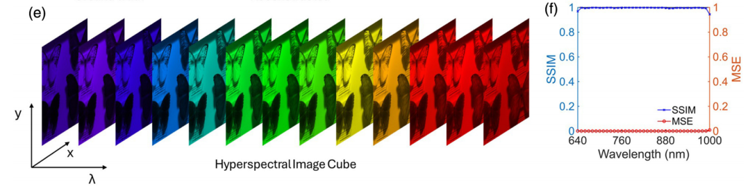
To verify the actual performance of the developed on-chip spectrometer in hyperspectral imaging, this study selected the publicly available butterfly hyperspectral dataset as the test object.This dataset covers a wavelength range of 420-1000nm and contains 59 spectral channels (spectral spacing of 10nm).It is provided in the form of a cube of three-dimensional hyperspectral images with a spatial resolution of 512×512 pixels.
Since the external quantum efficiency response of the experimentally fabricated devices is mainly concentrated in the 640-1000 nm range within the data acquisition range, this study used the spectral responses of 16 photodiodes with different photon trapping surface structures (PTSTs) in this wavelength band for reconstruction. First, the original dataset was interpolated to 361 wavelength points spaced 1 nm apart within the 640-1000 nm range, and then coupled with the simulated spectral responses of the photodiodes to generate corresponding photocurrent data. Finally, the data was input into a trained neural network model to reconstruct the hyperspectral image.
The network training phase used a synthetic dataset containing over 500,000 Gaussian spectra with varying peak values and widths, and model performance was evaluated using independent validation sets. As shown in the figure below, researchers found that the hyperspectral images reconstructed based on the experimental spectral responses of 16 photodiodes in the 640-1100 nm near-infrared band were visually highly consistent with the ground truth.
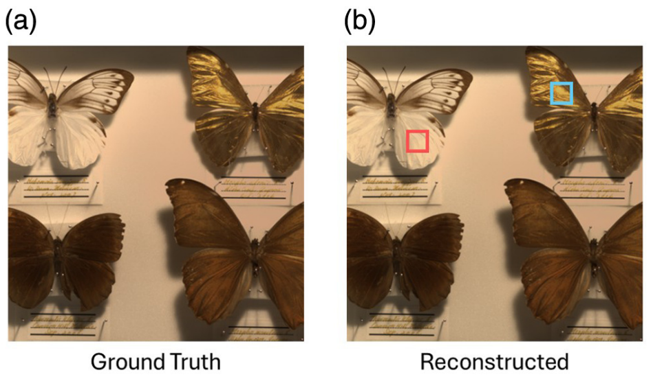
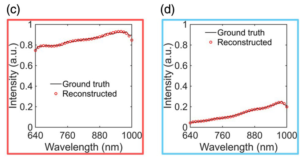
To further quantify the evaluation, this study selected two representative pixels from the image (as shown in the image above, marked with red and blue boxes respectively) for spectral comparison. As shown in the image below...The reconstructed spectrum matches the true spectrum well, accurately capturing the changes in the reflectance characteristics of butterfly pigments in the infrared band.
Building an AI-enhanced photon capture on-chip spectrometer
In this study, the core of spectral reconstruction is a specially designed fully connected neural network tasked with deriving the unknown incident spectrum from the photocurrent signal measured by the photodiode array. This is essentially a process of solving an inverse problem: due to the overlap in the detector's spectral responses, the system response matrix becomes ill-conditioned, making traditional direct inversion methods unstable and sensitive to noise. Neural networks, however, can learn to establish a robust mapping from the measured signal to the original spectrum, while naturally possessing denoising and regularization capabilities.
The network architecture consists of an input layer, four hidden layers, and an output layer.The input layer receives photocurrent signals from 16 photodiodes.The output layer directly outputs the reconstructed spectral data. The hidden layers use the ReLU activation function to introduce non-linearity, while the output layer employs a linear activation function. The network size (number of neurons) has been specifically optimized based on the complexity of the spectral data.The training used a large synthetic dataset containing over 500,000 simulated spectra.These spectra are composed of Gaussian curves with different peaks and widths to ensure that the model can learn a wide range of spectral morphologies.
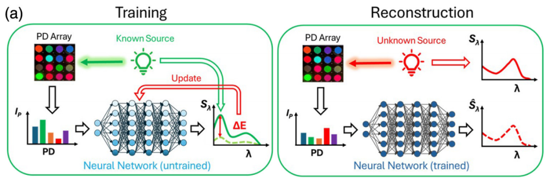
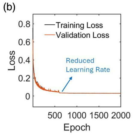
For the training strategy, the researchers used the Adam optimizer implemented based on the PyTorch framework. After testing various loss functions, a custom combined loss function that combines the root mean square error (RMSE) and the Pearson correlation coefficient (R) was ultimately selected. This function proved to be particularly effective in reconstructing narrowband spectra with sharp peaks. Specifically, the training batch size was set to 32, and the learning rate was 0.001.The researchers trained the model for 1,000 epochs and then reduced the learning rate to 0.0001 after the 600th epoch to promote better model convergence.To prevent overfitting, early stopping was used during training. As shown in the figure below, both training and validation losses decreased rapidly and eventually converged, indicating that the model learned well and had strong generalization ability.
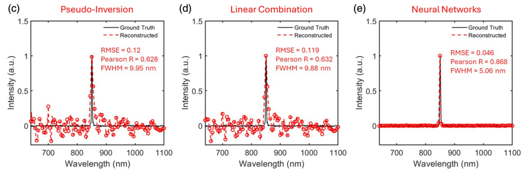
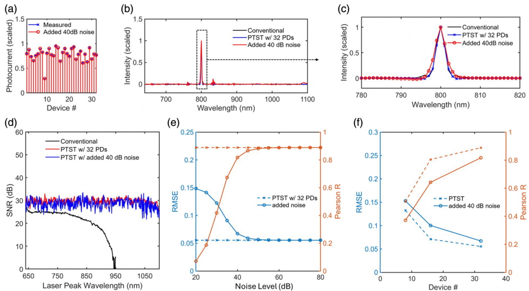
To verify the performance of this neural network, the researchers compared it with two traditional reconstruction methods. As shown in the figure below, the simple pseudo-inversion method and the method of linear combination of basis functions (such as Gaussian or sine functions) for the spectrum both performed poorly in reconstructing narrow linewidth laser spectra, with an RMSE of approximately 0.12 and a correlation coefficient R of approximately 0.63.
In contrast, neural networks are able to accurately capture sharp spectral features.The RMSE was significantly reduced to 0.046, and the correlation coefficient R was increased to 0.87.This result clearly demonstrates the superiority of neural networks in solving such inverse problems. They not only achieve higher reconstruction accuracy, but their inherent learning characteristics also make them more robust to noise interference.
A spectral resolution of 8 nanometers was achieved on 0.4 mm².
To fully verify the performance of the AI-enhanced on-chip spectrometer, this study conducted a series of experiments, focusing on evaluating the core role of the neural network model in spectral reconstruction and its actual performance.
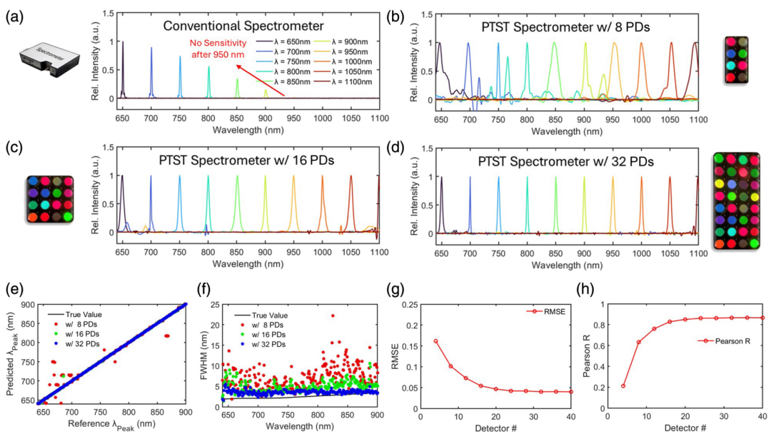
First, researchers tested the system's core detection capabilities using narrowband lasers. Experiments showed that the photodiodes integrating photon-trapping surface structures exhibited significantly improved sensitivity and signal-to-noise ratio in the 640-1100 nm wavelength range, particularly in the long-wave near-infrared region. Crucially, by inputting the responses of these detector arrays into a trained neural network, the system was able to accurately reconstruct the laser spectrum.When the number of detectors involved in the reconstruction increases to more than 16, the average error between the reconstructed spectrum and the reference true value drops to below 0.05, and the correlation coefficient exceeds 0.85.This verifies that the unique spectral encoding provided by the hardware and the analytical capabilities of the AI algorithm can work together effectively to achieve high-precision measurements.
Noise robustness is crucial for evaluating the performance of reconstruction algorithms. This study examines the robustness of the system by actively adding high-intensity simulated noise to real measurement data. The results show that even with additional noise up to 40 dB, the neural network model can still stably reconstruct a discernible spectral profile while maintaining an output signal-to-noise ratio of approximately 30 dB. This contrasts sharply with traditional methods, whose performance deteriorates drastically under noise.This highlights the powerful inherent regularization and noise suppression capabilities of the neural network employed.This is the key to realizing its practical application value.
To further demonstrate its potential for solving complex problems, the research applied the system to a hyperspectral imaging task. Using a trained neural network, the system successfully reconstructed a 512×512 pixel hyperspectral image cube from the open-source butterfly dataset using only the responses of 16 detectors. Finally, the researchers used mean squared error (MSE) and structural similarity index (SSIM) to quantitatively evaluate the overall reconstruction accuracy. Across all reconstruction wavelengths, the average MSE was as low as 2.3×10⁻⁴, and the average SSIM was as high as 0.9926.This demonstrates that the system possesses extremely high spectral fidelity, proving that AI can decode and reconstruct complex high-dimensional spectral spatial information from minimal hardware information.It has completed the leap from "point spectrum" to "spectral imaging".
Ultimately, this AI-enhanced spectrometer achieved a spectral resolution of 8 nanometers, a dynamic range of 50 dB, and a practical signal-to-noise ratio of 30 dB on a chip-scale (0.4 mm²) scale. Horizontal comparisons show that this system, co-built with intelligent algorithms and advanced photonics hardware, surpasses most similar miniaturized solutions in overall performance, marking a solid step towards the practical application of intelligent spectral sensing.
Miniaturized Spectral Sensing: Present and Future
Miniaturization and intelligent spectral sensing are becoming the forefront of global scientific research and industrial breakthroughs. In recent years, from basic research at top universities to application exploration by technology companies, a series of innovative cases have clearly demonstrated that embedding laboratory-level spectral analysis capabilities into chips and even everyday devices has entered a fast track of realization.
In academia, research is focused on fundamentally reshaping the form of spectrometers through disruptive photonic chip design and deep collaboration with artificial intelligence.A research team from Seoul National University in South Korea proposed a new scheme in Nature Communications.By using microcavities composed of plasma nanoparticles as filter arrays and combining them with machine learning algorithms, sub-nanometer spectral resolution was achieved at the micrometer scale.
Paper Title:Miniature computational spectrometer with a plasmonic nanoparticles-in-cavity microfilter array
Paper link:https://www.nature.com/articles/s41467-024-47487-y
at the same time,Scientists at the Swiss Federal Institute of Technology in Lausanne (EPFL) approached the issue from another crucial aspect of systems integration.A high-performance, precisely tunable erbium-doped waveguide laser has been successfully fabricated on a chip. This breakthrough, published in Nature Photonics, means that future integrated spectroscopy systems can expect a stable and high-quality on-chip light source, marking a solid step towards building a complete "laboratory on a chip."
Paper Title:A fully hybrid integrated erbium-based laser
Paper link:https://www.nature.com/articles/s41566-024-01454-7
Innovation in the industry is more market-oriented, focusing on transforming cutting-edge technologies into products and solutions that address real-world problems.Czech startup Iron Analytics launched the world's first portable Mössbauer spectrometer in 2025.Its revolutionary nature lies in the fact that it has successfully miniaturized the original 15-kilogram, 70-centimeter-long laboratory cabinet-style equipment into a portable device the size of a Coca-Cola can. This signifies that miniaturized spectroscopy technology is deeply penetrating from a consumer-end curiosity tool into core industrial fields, becoming a real productive force for improving production efficiency and process control.
In conclusion, the vision of miniaturized and intelligent spectral sensing is gradually being realized, with each piece of the technological puzzle being completed. However, true "embedding in everyday life" still faces practical challenges such as cost, reliability, and ease of data interpretation. Perhaps in the not-too-distant future, when spectral sensing modules can be mass-produced cheaply and reliably like today's cameras, our perception of the world will undergo a silent yet profound revolution. At that time, the "optical fingerprint" that interprets everything will no longer be the exclusive domain of laboratories, but will become another instinct for people to understand their surroundings.